
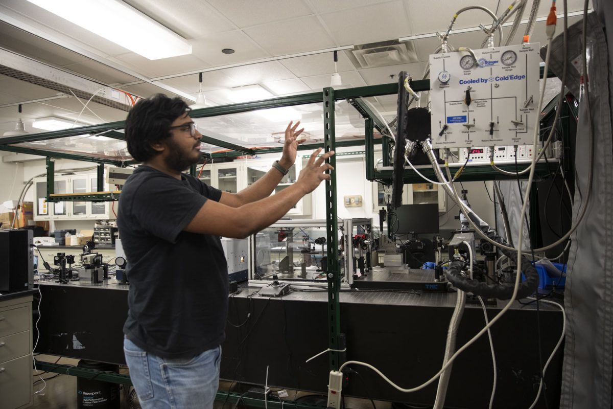
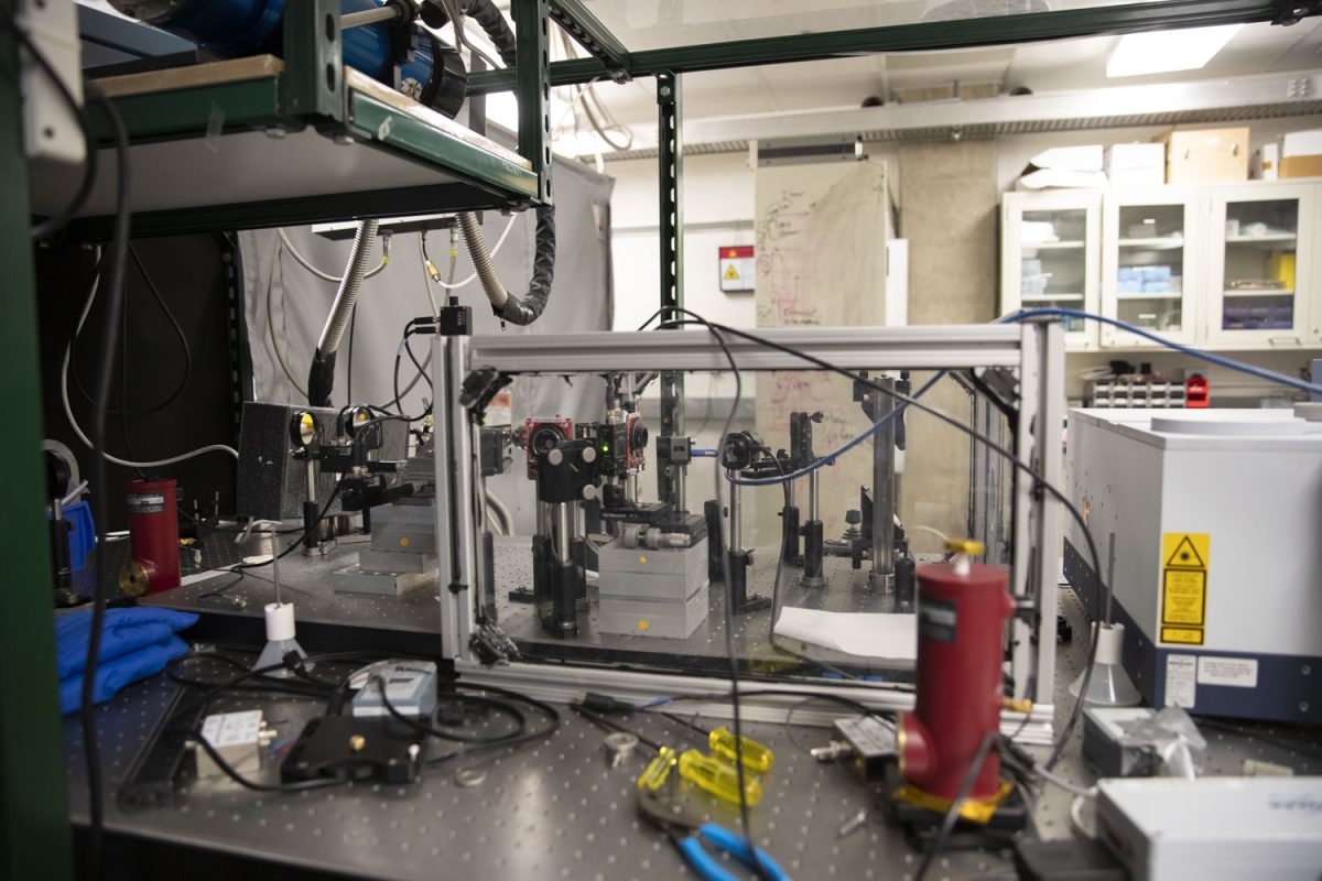
A team of researchers at the University of Iowa has created a new infrared cryo microscope.
The homemade microscope was created to enable the recent study aimed at deepening the understanding of material behavior, particularly, semiconductors at very low temperatures. This will aid in using different materials in a variety of technologies.
The study, titled “Determining the optical and polaritonic properties of isotopically pure hBN using cryogenic FTIR micro-spectroscopy,” observes the relationship between light and matter contained in electronic devices such as televisions, solar panels, smartphones, and more.
The research team was led by Thomas Folland, a professor of physics and astronomy at the UI, who said the study’s main goal was to use the specialized microscope to gain insights into the fundamental properties and behaviors of materials that can inform the development of new technologies.
“What we often do is take materials that have been made or that naturally exist, and then we try and kind of do experiments on them in order to understand what that behavior is and why it behaves that way,” Folland said.
Folland said the microscope will assist in a wide range of research, like allowing researchers to conduct experiments on materials at cryogenic temperatures down to the evaporation point of liquid helium, around negative 320 degrees Fahrenheit.
According to Folland, this will not only be a unique tool but also helpful in probing material properties. The microscope also uses reflective components instead of lenses, which enables it to work with infrared light that cannot pass through glass.
Folland said it provides a flexible, open-source, cost-effective alternative to commercial infrared microscopes.
In addition, Folland and his team have created instructions for others to create their own infrared cryo microscopes, which he hopes researchers will take advantage of.
“We’re actually hoping that people use it and find it interesting about how you actually build one of these things because that’s something that’s been kind of lacking,” Folland said.
Ultimately, the homemade design enabled the research group to customize and expand the microscope’s capabilities, such as adding to the ability to detect hardness in materials.
As he reflected, Folland said building and operating the microscope has served as an educational purpose, allowing students to gain hands-on experience with optics, alignment, and materials characterization techniques.
Maryam Vaghefi, a graduate research assistant at the UI, assisted in the research and is one of the co-authors of the study. Other co-authors include Eli Janzen and James Edgar, both from Kansas State University.
Vaghefi emphasized the importance of this research in both fundamental physics studies and commercial sensor and detector development.
“It helps a lot because the semiconductor material, some change with their temperature, so we like to know the properties of them when they go down in the different temperatures,” Vaghefi said. “We can also see more features, so it helps to improve the devices and know what specific temperature we can use that detector or sensor at.”
In addition, Vaghefi echoed that their designed microscope can be customized with various detectors and lenses, allowing for better resolution and temperature range studies.
“It can go down to 4K, so it gives us the ability to study the two-dimensional material in different temperatures and also nanodevices,” Vaghefi said. “Using the microscope, I can study the optical properties and see the sample from 20 microns to 200 microns, which is a very good resolution.”
Aditya Desai, a former student at the UI, assisted in reading and analyzing data collected from the microscope in the study.
RELATED: UI researchers complete TRACERS project for NASA
Desai specifically analyzed wide-bandgap semiconductors and Van der Waals materials by observing the data to identify material parameters and properties to understand how they will work with other materials or in devices.
According to the U.S. Department of Energy, “wide-bandgap semiconductor materials allow power electronic components to be smaller, faster, more reliable…”
On the other hand, Advadain describes Van der Waals materials as “the most important intermolecular force as they play a key role in the stability of all materials and chemical systems.”
“The materials are important because a lot of quantum technology that’s coming out requires you to know the cold materials and the optical properties because you can identify how you’re going to interact with light, which is the primary medium in which quantum technology works,” Desai said.
Despite switching from physics to law school, Desai credits his research experience with enhancing his critical thinking and problem-solving skills.
“When you’re analyzing data and not getting the results that you want, you have to adapt,” Desai said. “You have to handle adversity, persevere through it, and that ends up meaning that you develop a lot of critical thinking skills and a lot of problem-solving skills.”
Looking toward the future, Folland is looking forward to expanding the microscope’s capabilities to study chirality, which looks at how molecules interact with one another. The following steps look at adding new components to the microscope to enable this study and potential applications in fields such as pharmaceuticals and materials science.